
Phononic and Photonic Nanostructures Group (P2N)
Research Programme
Phonons in Nanostructures
As photons, phonons are excitations sensitive to reduced dimensionality, confinement and periodic fluctuations in the elastic and acoustic properties. In particular, the question of how energy and momentum relaxation is affected as sample dimensions become commensurate with the wavelength of excitations in solids, acquires increasing relevance since low dimensionality is intrinsically linked to energy discretisation. This, in turn, leads to dramatic changes in interactions involving lattice vibrations, compared to the usual case where a continuum of energies is available.
In analogy to photonic crystals, phononic crystals are inhomogeneous elastic media composed of one-, two- or three-dimensional periodic arrays of materials with contrasting elastic and or acoustic properties. They may be classified (2) into sonic bandgap crystals (1 m scale), phononic crystals (mm scale) and hypersonic crystals (um to nm scales). Our interest is the study of phononic crystals with periodic changes below one micrometer as well as acoustic cavities with characteristic length in the 10-100 nm, or nanophononics. Like photonic crystals, phononic crystals exhibit bandgaps and offer a rich physics to be explored including Anderson localisation, guiding and defect modes as well as anomalous tunnelling and slow wave phenomena.
Typical materials studied in nanophononics exclude semiconductors and the feature sizes are often in the mm and sometimes in the micrometer regime due to the formidable challenges presented by the realisation of test structures with feature size in the 1-50 nm range. If it were possible to describe in a model the interactions of confined phonons together with phonon filtering and focusing in a phononic crystal environment, then the choice of material with tailor-designed phononic properties could target the control of electron-phonon scattering mechanisms with implication in both electron mobility and thermal conductivity (3) . Likewise, the treatment of phononic crystals must include not only the band gaps, but also propagating guided modes and modes subjected to strong phonon focusing (4) or caustics (5).
Based on our previous work (6)(7)(8)(9)(10)(11) our first approach to the problem started in 2003 and was the experimental study of confined acoustic phonons in thin membranes of silicon-on-insulator (12), in other words, in an acoustic cavity, where the discrete spectrum of confined modes shifts to higher energies with increasing separation between levels as the membranes become thinner and thinner (Fig. 1a). During 2007 this work has been extended to simulations of low-frequency Raman Scattering of SOI structures (13) (Fig. 2) and the know-how being used to guide our work on thermal conduction in the nanoscale in the EU project NANOPACK.
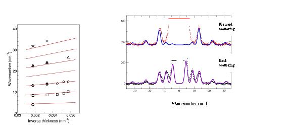
Figure 1. Frequencies of confined acoustic modes in SOI membranes as a function of the inverse of the membrane thickness (Sotomayor Torres et al, Phys. stat sol. (c) 1 (11) 2609-2612 (2004)).
Figure 2. Forward and back scattering of a 32.5 nm thick SOI membrane. The solid lines denote the simulated spectra and the dotted lines are the experimental ones (adapted from Sotomayor Torres et al, Phys. stat sol. (c) 1 (11) 2609-2612 (2004))
(2) J H Page, paper given at the PECSVI conference, Crete, 19-24 June 2005.
(3) D G Cahill et al, “Nanoscale thermal transport”, J Appl. Phys. 93 793 (2003)
(4) S Yang, J H Page, Z Liu, M L Cowan, C T Chan and P Sheng, Phys Rev Lett 93 024301-1 (2004)
(5) J P Wolfe, Imaging phonons: Acoustic wave propagation in Solids, Cambridge University Press, 1998
(6) M Watt, C M Sotomayor Torres, R Cheung, C D W Wilkinson, H E G Arnot and S P Beaumont, Raman Scattering of reactive ion etched GaAs, J Mod Optics 35 (3) 365-370 (1988)
(7) H Benisty, C M Sotomayor Torres and C Weisbuch, An intrinsic Mechanism for the poor luminescence Properties of Quantum Box Systems, Phys Rev B 44 (19) 10945-10948 (1991). Reprinted by SPIE in its Milestone Series, Volume MS180 in: Selected Papers on Semiconductor Quantum Dots, Editor: Frank W. Wise, pp 344-347 (2005)
(8) H Qiang, F H Pollak, C M Sotomayor Torres, W E Leitch, A H Kean, M A Stroscio, G J Iafrate and K W Kim, Size dependence of the thermal broadening of the exciton linewidth in GaAs/Ga0.7Al0.3As single Quantum Wells, Appl Phys Lett 61 (12) 1411-1413 (1992)
(9) W S O Rodden, C M Sotomayor Torres and C N Ironside, Three Dimensional Phonon Confinement in CdSe Microcrystallites in Glass, Semicond Sci Technol 10, 807-812 (1995)
(10)P D Wang C Cheng, C M Sotomayor Torres and D N Batchelder, “GaAs micrometer-sized dot imaging by Raman Microscopy”, J Appl Phys 74 (9) 5907-5909 (1993)
(11) J P Leburton, J Pascual and C M Sotomayor Torres (Eds), Phonons in Semiconductor Nanostructures, NATO ASI Series E Vol 236, Kluwer Publishing, The Netherlands, 1993
(12) C M Sotomayor Torres, A. Zwick, F Poinsotte, J Groenen, M Prunnila, J Ahopelto, A Mlayah and V Paillard, “Observations of confined acoustic phonons in silicon membranes”, Physica status solidi (c) 1 (11) 2609-2612 (2004).
(13) J Groenen, F Poinsotte, A Zwick, C M Sotomayor Torres, M Prunnila and J Ahopelto, Inelastic Light scattering by longitudinal acoustic phonons in thin silicon layers: from membranes to silicon-on-insulator structures, to appear in Phys Rev B, 15th January 2008, 77 (4).
Nanofabrication
In our group we work on three nanofabrication methods and combinations thereof, as well as researching new metrology methods for 50 nm patterning.
Electron beam lithography (EBL), using a tightly focused beam of electron to expose a resist, crosslink it thereby leaving a nanopatterned polymer behind after developing, which is used as a mask of for lift off. In some cases it is used for direct writing. We use EBL primarily for writing patterns for nanoimprint lithography stamps, to pattern Si, SOI, SiO2, polymer films or mesoscopic particles.
We have used EBL to write a lattice of defects in a layer of a 2D photonic crystals and to write deterministic defects. Examples are shown in Figure 3.
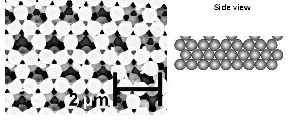
Figure 3. Left: Scanning electron micrograph of a 2D triangular defect layers inscribed on the top layer of a 3D PMMA opal by electron beam lithography. Right: side view of the left-hand side structure (G Kocher et al, in preparation).
Nanoimprint lithography (NIL) (14) is basically a polymer surface structuring method by making a polymer flow into the recesses of a hard stamp in a cycle involving temperature and pressure. It has been said to be among the top 10 technologies which will change the world (15). To nanoimprint a surface, three basic components are required: a stamp with suitable feature sizes, a material to be printed and equipment for printing with adequate control of temperature, pressure and control of parallelism of the stamp and substrate. The NIL process is illustrated schematically in Figure 7.1. In essence, the process consists of pressing the solid stamp using a pressure in the range of about 50 to 100 bar, against a thin polymer film. This takes place when the polymer is held some 90 to 100 °C above its Tg, in a time scale of few minutes, during which the polymer can flow to fill in the volume delimited by the surface topology of the stamp. The stamp is detached from the printed substrate after cooling both the stamp and substrate. There are several variations of NIL, including single-step thermal NIL and Step-and-Stamp Imprint Lithography (SSIL). Our group has contributed to the development of the former approach for nearly 10 years and will start activities in SSIL at CIN2 using the recently acquired NPS300 tool. One of the key contributions of our group has been in the area of 3D NIL but using a combination of methods (thermal and UV NIL) and realising structures consisting of three layers of nanoimprinted polymers. This method has been called Reverse contact UltraViolet Nanoimprint Lithography (RUVNIL) (16) and was inspired by the work of the Ann Arbor group led by Prof S. Pang (17). In this process, a UV cross-linkable polymer and a thermoplastic polymer are spin coated onto a patterned hybrid metal-quartz stamp. These thin polymer films are then transferred from the stamp to the substrate by contact at a suitable temperature and pressure. The whole assembly is then exposed to UV light. After separation of the stamp and the substrate, the unexposed polymer areas are rinsed away with a suitable developer, leaving behind the negative features of the original stamp. The process is shown schematically in Figure 4. By using the same UV-curable polymer for each layer three-dimensional nanostructures have been obtained. This technique offers a unique advantage over Reverse contact NIL and thermal NIL, as no residual layer is obtained by controlling the UV light exposure, thus avoiding the usual post-imprinting etching step, therefore leading to much better control of critical dimensions. In another study, the printed polymer was treated so at to bind selectively polymer brushes (18), which can be used to build supramolecular structures.
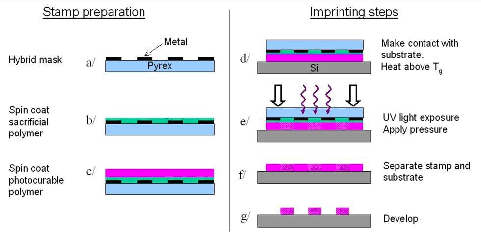
Figure 4. Schematics of the Reverse UV Nanoimprint Lithography. Then left sequence shows the steps to fabricate a mould, while the right process sequence illustrates the RUVNIL steps. (N. Kehagias et al. Nanotechnology 18, (2007) doi:10:1088/0957-4484/18/17/175303).
(14) C M Sotomayor Torres, the book Alternative Lithography: Unleashing the Potentials of Nanotechnology (Ed.: C. M. Sotomayor Torres), Kluwer Academic Plenum Publishers, New York, 2003
(15)MIT Technology Review, February 2003, 33.
(16)N. Kehagias, M. Zelsmann, K. Pfeiffer, G. Ahrens, G. Gruetzner and C. M. Sotomayor Torres, J. Vac. Sci. Technol. B 2005, 23, 2954. N. Kehagias, V. Reboud, G. Chansin, M. Zelsmann, C. Jeppesen, C. Schuster, M. Kubenz, M Kubenz, F. Reuther, G. Gruetzner and C. M. Sotomayor Torres, Reverse- contact UV nanoimprint lithography for multilayered structure fabrication, Nanotechnology 18, (2007) doi:10:1088/0957-4484/18/17/175303.
(17) L.-R. Bao, X. Cheng, X. D. Huang, L. J. Guo, S. W. Pang, and A. F. Lee, J. Vac. Sci. Technol. B 2002, 20, 2881.
(18) A Genua, J A Alducin, J A Pomposo, H Grande, N Kehagias, V Reboud, I Mondragon, C Sotomayor and D Mecerreyes, Functional patterns obtained by nanoimprint lithography and subsequent growth of polymer brushes, Nanotechnology 18, 215301-215307 (2007).
Self-assembly of colloidal particles. In our group we have pioneered, together with our collaborators at the Technical Research Centre of Finland, a method to grow photonic crystals of PMMA and silica spheres on patterned Si and SOI substrates, with recesses up to 10 um deep using vertical and lateral capillary forces (19) . The combination of Si technologies and self-assembly opens several avenues for heterogeneous integration of optical, chemical and mechanical structures made out of colloids with Si-based electronics (20). A variation of this technique is acoustic field-induced self-assembly, which we developed to improve the long-range order of colloid-based photonic crystals. This has resulted in extremely well ordered structures (see Figure 5) with unparallel internal order as demonstrated by transmission and diffraction measurements (21) which will be used for light propagation and emission studies.
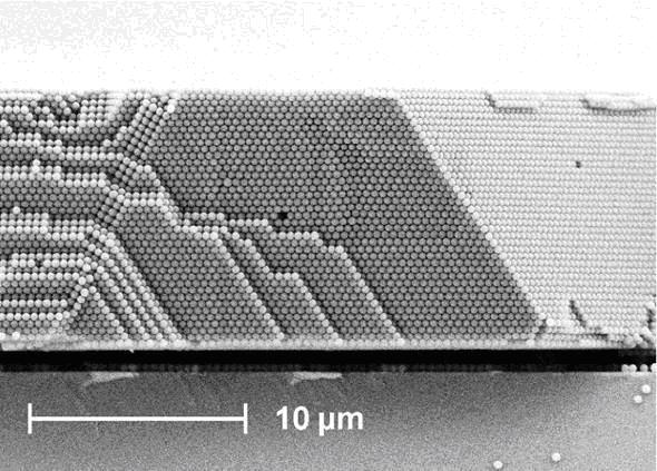
Figure 5. Scanning electron micrograph of a 3D photonic crystals grown under the influence of an acoustic field (W. Khunsin et al. in preparation).
(19) Finnish patent application FI20075153 “Capillary transport of nanoparticles or microparticles to forma and ordered structures” (20)G.. Kocher, W. Khunsin, S. Arpiainen, J. Romero-Vivas, S. G. Romanov, J. Ye, B. Lange, F. Jonsson, R. Zentel, J. Ahopelto, C. M. Sotomayor Torres, Towards Si-based photonic circuits: integrating photonic crystals in Silicon-on-Insulator platforms, Solid-State electronics 51, 333-336 (2007)
(21)W. Khunsin, G. Kocher, S. G. Romanov, C. M. Sotomayor Torres, Quantitative characterisation of opal lattice perfection, submitted for publication.
Nanopatterning Metrology is an essential component of nanofabrication. While scatterometry (22) is an excellent approach (23) , alternatives are needed to compare for in-line monitoring of printed quality down to 50 nm features, first in terms of presence, deformation and structure peel off when demoulding. In this context, we are developing a method based on diffraction from a test structure in the form of an asymmetric grating to detect defects by comparing peak position and intensities in the diffraction spectrum (24). For larger printed structures a fruitful collaboration with the ETH Zuerich team of Dr Jacqueline Vollmann, whose expertise is in acoustic reflection spectroscopy is proving to be highly complementary (25). To monitor and simulate the thickness of the residual layer and the possible bending of the wafer in single-step printing, a coarse-grain model has been developed within the NaPa project by Drs S Zaitsev, V. Sorotin Nad A. Svintsov of the Institute of Microstructural Technologies (Chernogolovska, Russia) with experimental support from our team. Its accuracy and simplicity makes it ideal for in situ-monitoring.
(22) D. Fuard, C. Perret, V. Farys, C. Gourgon and P. Schiavone, J. Vac. Sci. Technol. B 2005, 23, 3069.
(23)C Gourgon, N Chaix, H Schift, M Tormen, S Landis, C M Sotomayor Torres, A Kristensen, I Fernandez-Cuesta, D Mendels, L Montelius and T Haatainen, Benchmarking in thermal nanoimprinting of 50 nm features, submitted to J Vac Sci Technol B.
(24) T Kehoe, V Reboud, N Kehagias, S Landis, C Gourgon and C M Sotomayor Torres, Sub-wavelenght diffraction for characterisation of nanoscale features, SPIE , to appear in Proc of Microlithography 2008, to be held in February 2008, San Jose, CA, USA.
(25) J Bryner, J Vollmann, L Aebi, J Dual, T Kehoe and C M Sotomayor Torres, paper Nr PID516652, presented at Ultrasonics 2007.
Photonic Nanostructures
Light propagation in 3D opal-based photonic crystals. The interest in 3D photonic structures is based on the need to understand light propagation and light emission in nanostructured matter. It is widely acknowledged that 3D photonic crystals hold the key to thresholdless emission processes due to the absence of competing modes if the emission occurs at a frequency in the gap overlapping a well-defined defect mode. In practice, the demands are very stringent, including a defect-free 3D photonic crystal in the scale of the Bragg length, a well defined bandgap and suitable in- and out-coupling mechanisms. The presence of interfaces is virtually unavoidable and theoretical and experimental methods are few (26). We have concentrated in, for example, the angle-dependent study of transmission in triple-film opals, which has shown that the interfaces are responsible for the polarisation anisotropy and the narrowing of the transmission minima (27). To date, there is no simulation which can be used to test these results.
(26) G Qiu, K Vynck, D Cassagne and E Centeno, Optics Express 15 (6) 3502-3506 (2007).
(27) W Khunsin, S G Romanov, R Zentel and C M Sotomayor Torres xxx, Non-additive transmission in triple-film opals, submitted for publication.
Plasmon-photon coupling in 2D polymer-based printed photonic crystals.One of the attractions of NIL is the patterning of functional polymers into-device-like structure both, to test the quality of the NIL process and to explore application potentials. In previous work we showed how dye-loaded (28), as well as quantum dot-loaded (29), printed polymer 2D photonic crystal structures exhibited a 2x to 3x enhancement of the extraction efficiency compared to unpatterned loaded polymer layers. The plasmon-photon interaction was used to demonstrate a factor of 27x enhancement in a structure containing a rough Au film at the base of the doped polymer 2D PhC (30) as shown if figure 6. This result is likely to impact the printable photonic struxtures for lab-on-a-chip and similar application where light detection normal to the surface is needed.
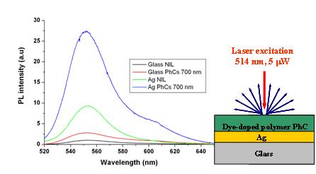
Figure 6. Photoluminescence spectra of a Rhodamine 6G/mr-NIL 6000 printed on glass (dark blue), nanoimprinted with PhCs (red blue), nanoimprinted on a Ag film (green line), nanoimprinted with PhCs on a Ag film (blue blue). The emission shows a 27-fold enhancement observed for the Ag coating + PhCs with respect to that of the nanoimprinted unpatterned substrate. The inset denotes the experimental configuration (V. Reboud et al. Optics Express 15, 7190 (2007)).
(28) V Reboud,et al 2d phc with dye
(29) N. Kehagias, V. Reboud1, M. Zelsmann, M. Striccoli, M. Tamborra, M. L. Curri, A. Agostiano, M. Fink, F. Reuther, G. Gruetzner and C. M. Sotomayor Torres, Spontaneous emission of nanocrystals in nanoimprinted photonic structures, submitted to Microelectronic Engineering.
(30) V. Reboud, N. Kehagias, M. Zelsmann, C. Schuster, M. Fink, F. Reuther, G. Gruetzner and C. M. Sotomayor Torres, Photoluminescence enhancement in nanoimprinted photonic crystals and coupled surface plasmons, Optics Express 15, 7190 (2007).
Band-edge printed polymer lasers. Another type of optical device-like structure designed and tested was a visible wavelength band edge laser fabricated by NIL in dye chromophore-loaded polymer. High-symmetry band-edge modes are used to generate laser emission. The experimental lasing frequencies are in good agreement with the one calculated using a two-dimensional plane-wave algorithm. The optical pump threshold power was better than previously reported data (31). These results demonstrate the potential of nanoimprint lithography for the fabrication of two-dimensional planar photonic crystal structures in an active medium in a scalable one-step process.
(31) V. Reboud, P. Lovera, N. Kehagias, M. Zelsmann, C. Schuster, F. Reuther, G. Gruetzne
Inorganic nanostructures
The driving force of research in these structures is the wealth of properties that can be potentially engineered by suitable choice of a matrix in, e.g., lamella, 1-D, spherical, star-like form, spacers and intercalation material. As a first step, in collaboration with the Universidad de Chile and the Universidad Tecnologica de Santiago, we singled out the understanding between synthesis procedures and resulting structures. We focused on VO5 and MoS2 as matrices for their promise as optical and electronic material, respectively. Moreover, we successfully investigated also rare-earth doped lanthanides for improved light emission characteristics. Among the most striking finding was the follow up of the discovery of the unusually high surface area nano-urchin of VO5 (32), shown in figure 7, which help to unravel the rolling mechanism of lamellar structures into tubes, rods, nanourchins. Furthermore, the prospects of introducing Au nanoparticles in these structures was explored and demonstrated (33). Likewise, the introduction of CdS quantum dots in MoS2 lamellas was also studied. The latter showed that while the optical properties appeared very promising the high defect density pre-empted the tracking of enhanced optical emission, expected from the regular spacing and co-operative phenomena (34). This work is in its infancy and much is expected from the combined advantages of nm control of the material size, shape and surface as well as from the seemingly endless range of properties.
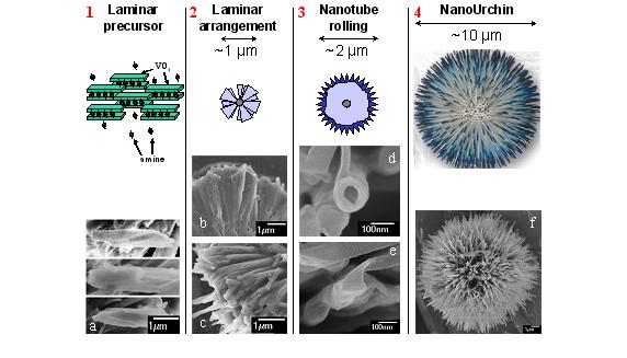
Figure 7. Schematics of the formation of nanourchins of VO5 from an intercalated lamella (adapted from C. O’Dwyer et al. Chemistry of Materials 18, 3016 (2006).
(32) C. O’Dwyer, D. Navas, V. Lavayen, E. Benavente, M. A. Santa Ana, G. Gonzalez, M. Schmidt, S. B. Newcomb and C. Sotomayor Torres, Nano-Urchin: The Formation and Structure of High Density Spherical Clusters of Vanadium Oxide Nanotubes, Chemistry of Materials 18, 3016- xxx (2006). Featured cover article.
(33) V. Lavayen, C. O'Dwyer, M. A. Santa Ana, N. Mirabal, E. Benavente, G. Cardenas, G. Gonzalez, and C. M. Sotomayor Torres, Functionalization of Lamellar Molybdenum Disulphide Nanocomposite with Gold Nanoparticles, Appl. Surf. Sci. (2006) doi:10.1016/j.apsusc.2006.07.039.
(34) C. O'Dwyer, V. Lavayen, N. Mirabal, M. A. Santa Ana, E. Benavente, S. Ormazabal, G. Gonzalez, Z. Lopez, O. Schöps, U. Woggon, C. M. Sotomayor Torres, Surfactant-Mediated Variation of Band-Edge Emission in CdS Nanocomposites, Photon. Nanostruct. Fundam. Appl., 5, 45 – 52 (2007).
Resources and Collaborations
The Phononic and Photonic Nanostructures group
The group is led by Prof Dr Clivia M Sotomayor Torres, an ICREA research professor. Mr Michael Schmidt is the graduate laboratory Engineer. Dr Gudrun Kocher is the postdoctoral researcher working in the NANOPACK project. Drs Vincent Reboud, Nikolaos Kehagias and Timothy Kehoe are currently working in the NaPa project and will later work in the NaPANIL project, Mr John Cuffe holds an Irish Research Council for Science Engineering and Technology PhD studentship, supervised jointly with Prof John McInerney at University College Cork and by the P2N head and works in the NANOPACK project.
Projects
The group is partner of the following projects:
Nano Packaging Technology for Interconnect and Heat Dissipation (NANOPACK), a large-scale Integrating Project of the EU-FP7 ICT theme, addressing one of the major limitations to continued performance increases in the semiconductor and power electronics industries, namely, integration density and thermal management. It will develop new technologies and materials for low thermal resistance interfaces and electrical interconnects by exploring nanotubes, nanoparticles and nano-structured surfaces using different enhancing contact
Formation mechanisms combined with high volume compatible manufacturing technologies. NANOPACK started on 1st November 2007. The group is committed to basic research in thermal conductivity and confined acoustic phonons.
Nanopatterning, Production and Applications based on Nanoimprinting Lithography (NaPANIL), a large-scale project of the EU-NMP theme, which aims to develop processes, materials and tools, both for manufacturing and for control, for truly 3-dimensional nanosurfaces with feature dimensions ranging from 50 nm to several m. The nanosurfaces will be realised using various variants of nanoimprinting lithography. The dedicated application is to control light at nanostructured surfaces and a few potential high impact products have been identified by the end-user partners in the consortium. Design, demonstration and prototyping these applications will act as test bench for the new manufacturing paradigm. The manufacturing processes envisaged possess generic aspects for production of any kind of topographically 3-dimensional nanostructured surfaces.
NaPANIL is expected to start on 1st March 2008.
COST Action MP0702: Towards functional sub-wavelength photonic structures. www.cost.esf.org/index.php?id=1559
The objective of the Action is to establish active links between European laboratories working in the field of artificial materials for photonics applications, where the structural dimensions are at or below the wavelength of light. Fabrication of such structures has become possible due to the expertise delivered by nanotechnology, which opens the way to the study of new functional artificial materials and plasmonic structures, promising progress in miniaturisation - and which will allow exploration of new aspects of light-matter interaction. The goal is to increase knowledge about the basic mechanisms of the interaction of light with matter on a sub-wavelength scale. The scientific innovation concerns: the basic mechanisms of light-matter interaction in micro- and nanostructured materials - including metals (plasmonics), the trade-off between strong localization and propagation losses, photonic diagnostic instruments, and non-linear effects. The technological impact of the Action will lead to the implementation of advanced optical equipment and devices with high performance and low cost. The scientific transformation resulting from the Action will facilitate interconnection between topics that will produce new results in the field of photonics and pave the way to the forthcoming "era of nanophotonics".
Keywords: Nanophotonics, non-linear nanophotonics, hybrid material systems, plasmonics, metamaterials.
This actions starts in 2008.
Collaborations
Several collaborations are going on with project partners. Among these, the ones with the teams of Prof J Ahopelto (VTT, Finland), Prof G Gonzales (U de Chile), Prof E Benavente (U Tecnologica de Santiago, Chile), Dr Stefan Landis (LETI, France), Dr M Zelsmann (CNRS-LTM, France), Prof L Chi (U Muenster, Germany), Prof N Lu (Jilin University, China), Prof L Curri (Bari, Italy), Dr D Mecerreyes (CIDETEC, Spain), Ms Gabi Gruetzner (mrt GmbH, Germany), Prof A Eychmueller (U Dresden, Germany), Dr S Zaitsev (IMT, Russia), Dr Simon Newcombe (Geble Scientific Ltd, Ireland) and Prof R Zentel (U Mainz, Germany) have been particularly fruitful.
It is intended to establish strong links with colleagues at CIN2 in the near future, once the P2N group is housed in CIN2 premises.